In a synchronous bus, a common clock is shared between the CPU interface and the peripherals. Thus, one of the control signals in the synchronous bus will be the clock.
The transactions on a synchronous bus are timed relative to the edges of a clock signal, with each read/write transaction finishing within one cycle.
- At the end of the cycle, the transaction is assumed to be complete as there is no feedback from the peripheral to the controller with this type of bus.
- A successful transaction is assumed, but there is no mechanism to verify this.
- There is also no mechanism to change the rate of transfer.
A second read/write or R/W control line indicates the type of transaction being executed.
- Following convention, the name “R/W” (read not write) indicates the mode is being set to read when a signal is a 1, and a write when this signal is a 0.
A block diagram of a system where the processor is the only controller on the bus is shown below. The system uses a centralized address decoder to determine which device is involved in the transaction. Centralized vs. de-centralized doesn’t really matter; any data source source that can drive the data lines must only selectively drive those lines, to prevent conflicts. For the system bus, tri-state drivers are used between the output of all potential data sources and the shared data lines.
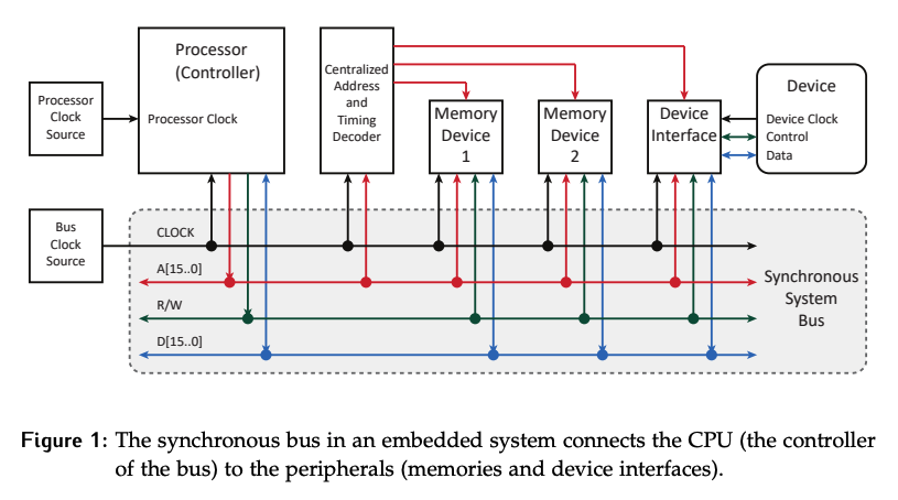
The synchronous bus model used in this course has the following signals:
- Clock signal (
CLOCK) - Address bus signals (
A[15..0]) - Data bus signals (
D[15..0]) - Read/write signal (
R/W)
Note that memory and device interfaces can read the address and control lines, but can only write the data lines. The CPU controls the value on the address lines, A[15..0], and R/W. The clock comes from an external source.
Read Transaction
Every read transaction follows the same form:
- Controller gets control of the bus
- Controller drives the address and indicates that the transaction is a read
- Peripheral recognizes that it is involved in a read transaction
- Peripheral retrieves data from the indicated address and drives it on the data lines
- Controller receives and stores the data.
Consider the timing of a synchronous read transaction as shown in Figure 2.
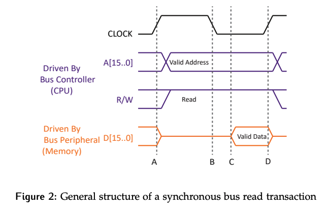
Controller Phase
The rising edge of the clock (aka controller edge) is marked as time in the diagram. This edge tells the controller (the CPU) to start the transaction by providing the address and the transaction type.
- In this case, pulling the
R/Wline to 1 indicates a read.
There may be some delay between time and the values on these lines being set, but the changes must be early enough that the values are stable at the furthest device when the falling edge of the clock comes. Since only the controller manipulates bus lines while the clock is high, this time period is referred to as the controller phase.
Peripheral Phase
The falling edge (aka peripheral edge) is marked as time . It marks the start of the peripheral phase, which is the part of the cycle when the clock is low.
After the falling edge, the first thing that needs to happen is the address needs to be checked to determine which device or memory is to be read from, and which specific piece of data within the peripheral is being requested. This is done by using centralized address decoding to select the device, and internal logic to identify the specific source.
Once the target location is known, the device retrieves the desired information and places it on the data lines, as marked by time . It must be possible for the device to place the data on the lines and for the values to be stable at the input of the MDR before the next rising edge, which is marked as time .
Write Transaction
Every write transaction follows the same form:
- Controller gets control of the bus
- Controller drives the address and indicates that the transaction is a write
- Peripheral recognizes that it is involved in a write transaction
- Peripheral prepares to store the data
- Controller receives and stores the data
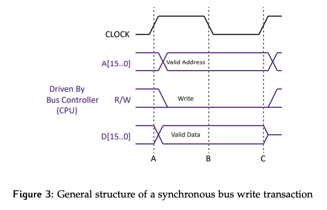
Like read transactions, the CPU starts off by driving the address the write signal on the bus. Unlike the read case, the CPU is in possession of the data to be written. This data will be driven to the data lines at the same time as the address and control information are driven to the bus.
At time , we enter the peripheral phrase: The address is checked to determine which memory/device is involved and which specific location the information should be written to. Once this is determined, any necessary logic to route the value to the input of the destination will be triggered. The data will only be clocked into the destination on the next rising edge at time .