Unidirectional Read
A unidirectional read port is only able to read from one register. This is suitable for interfacing with a simple, persistent data source such as a switch.
The ideas in this section are applicable to any read-only register, such as the status register SR and Data In DI. In terms of the hardware required, and the transaction from the CPU’s perspective, the only difference between the two registers is their address.
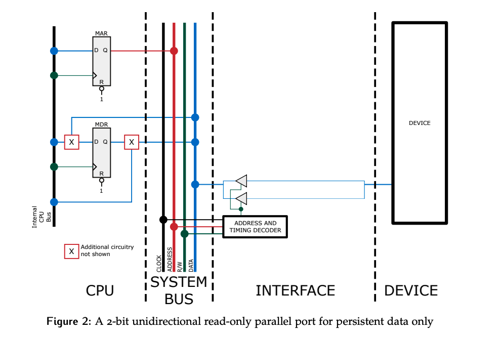
The device directly provides data to the input of the tri-state buffers.
- The number of buffers is determined by the width of the data lines on the system bus, as there will be one driver per line.
- All of the buffers are controlled by a single control signal, which is generated by the device based on the control lines of the system bus, the address and timing signals such as clock.
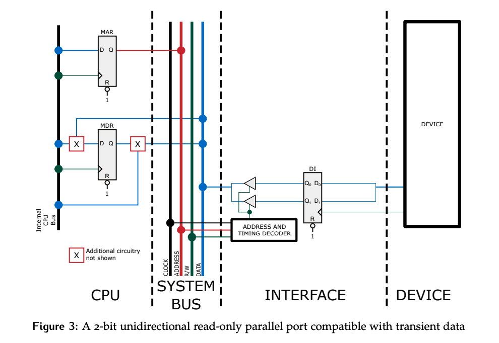
Transient Data / Buffering
What if we want to connect a read-only device where the data is not persistent?
In this case, we need to buffer or store the data so that it is guaranteed to remain stable for the duration of the read transaction. This can be implemented in hardware by adding a register between the data source and the tri-state connected to the system bus. This is shown below.
Device Connection
How do we connect the parallel port interface and the device?
The simplest way is to use a switch. While the input data does change depending on the switch position, the timescale of that change relative to a bus cycle means the data can be treated as persistent.
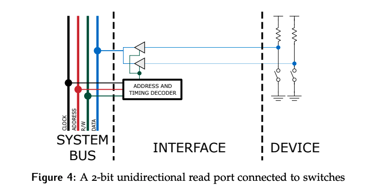
The input should always be digital (logic 1 or logic 0). Thus, if a pull-up resistor is not used, the input line would be floating when the switch is open. In this configuration, the input will be logic 1 when the switch is open, and logic 0 when the switch is closed. If we want the opposite behavior, the positions of the switch and resistor can be swapped.
Unidirectional Write
A unidirectional write port can only write to one register. This is suitable for interfacing with a simple output device, such as an LED. The hardware for this is shown below.
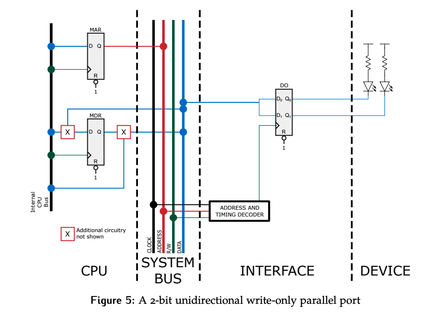
Data from the MDR is made available on the data lines of the system bus, while the MAR places the address of the register to be written to on the bus. At the appropriate time in the bus transaction cycle, a WriteClk signal is used to clock the data into the target register. Now that the data is contained in the register, it can be used by the device.
- One common scenario is using LEDs as state indicators. Each output of the register in the figure above is used to control a single LED. This is just a simple example.
Timing
The timing for a synchronous write is shown below.
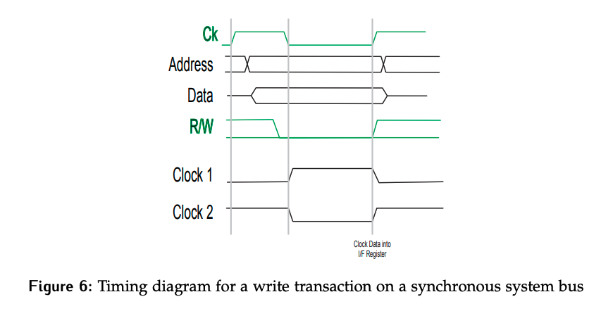
The clock signal feeding the DO register will be generated by the address and timing decoder with timings matching those shown by “Clock 2” in the figure.
Note that the timing shown by the “Clock 1” signal would not give the desired behavior, as the data would be clocked into DO on the peripheral edge of the bus clock, not at the end of the period. To understand the logic implemented within the address and timing decoder to produce a signal similar to Clock 2, let’s consider the conditions required for data to be loaded into DO:
- The bus clock should be in the peripheral phase
- The address on the bus is that of the
DOregister - The control line indicates the transaction is a write
Writing these as a logical relation would result in Clock 1:
The result is a signal with a falling edge where there should be a rising edge. We can fix this by inverting the signal: