What issues could prevent a synchronous bus transfer from working reliably?
A read operation requires that a location in a device interface or memory be accessed and that the value is copied into the CPU. This is shown in 2 views by the ladder diagram and timing diagram below.
Ladder Diagram
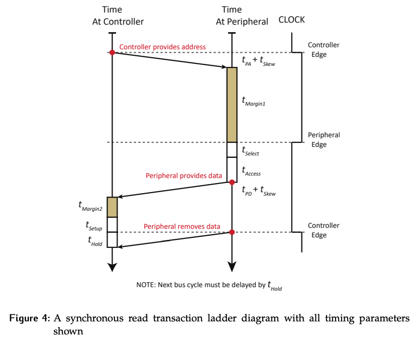
Controller Phase
As shown in the ladder diagram, the read transaction begins on the controller (rising) edge of the clock signal. The controller edge is the signal for the CPU to put the address and control (R/W) information on the bus. These values aren’t immediately available, as real wires have some propagation delay for a signal to change. Some timing parameters we have to consider:
- Address propagation delay (): Time for change in an address to propagate from the controller to all potential peripherals.
- Skew time (): Difference in signal propagation times between the multiple signals we have. Even if all the data lines on the bus are changed at the exact same time, they will not arrive at the destination at the same time due to small differences in parasitics.
- Only applicable to multi-line bus signals (address and data)!
- Margin time () : Any extra time after propagation and skew time.
Peripheral Phase
The falling edge marks the transition into the peripheral phase. This signals to the centralized address decoder (or devices in decentralized case) that address and control information on the bus are stable and can be acted on.
Timing parameters we need to be aware of:
- The first action is figuring out which device is involved; with a centralized address decoder, this is where address signals get processed through the combinational logic to assert one enable or chip select signal. This is the select time ().
- Separately, we need to determine the transaction type, then go to the specific location and retrieve the data. This is called the access time (), and happens immediately after the device is selected.
- Just like the address, the data values must propagate, so there is a data propagation delay time (). For a bus, this is defined based on the worst case propagation time between any data source and receiver in this system. This differs from the definition of address propagation; while any device can drive data, only the controller can set the address.
- Since there are multiple data lines, they will also experience skew.
Some additional margin time is often added after the data is stable at the controller to provide some cushion, in case the select, access, propagation or skew time become larger than the spec as the system ages or is subject to different conditions. Margin time is required because in real systems, there will always be some extra time in case the system doesn’t perform exactly as expected.
Data Save
The end of the cycle is the next rising edge. Here, the data that was read will be clocked into the MDR. Why wait until the controller edge instead of doing this as soon as data is available?
- Reason 1: Having margin time is important.
- Reason 2: The synchronous bus uses set triggers for actions. Different devices will take different amounts of time to respond, so how would the CPU know the data was ready to be clocked in? It can’t know without adding more control signals. Instead, the next controller edge, which is already available, is used as a trigger.
- This is an example of a virtual
MFC(memory function complete) signal.
- This is an example of a virtual
Since the MDR is a register built from flip-flops, metastability is a concern; thus, we need to observe setup () and hold times.
On the peripheral side, seeing the rising edge means it can stop driving data on the bus. Turning the data off at the edge typically makes the assumption that the hold time is less than the propagation time, which is usually true.
Timing Diagram
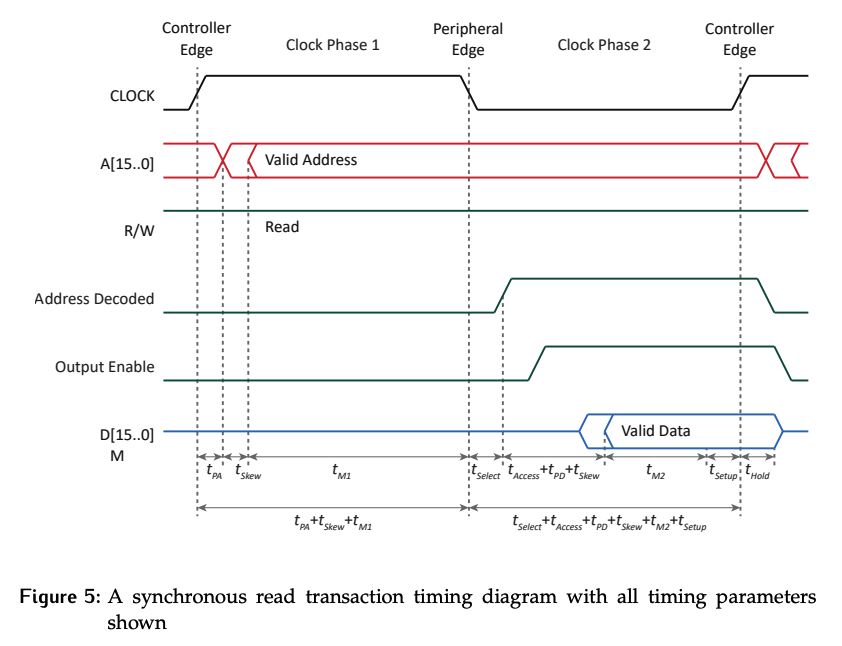
This view provides insight into the signals themselves, such as Address Decoded and Output Enable.
Address Decodedasserts that the device is now aware of its involvement in the transaction. This is a generic name that could represent the chip select or enable signal from a centralized decoder, or the output of a decoder inside the device interface.
Output Enable is the control signal of the tri-state connecting the data from the device interface to the system bus. It will be generated by the register selection unit inside the device interface and is driven by the logic combination: Transaction is in peripheral phase (clock is low), the register’s address is present, the transaction is a read. This can be written as: