Integrated DMA is an implementation of DMA. It allows the device interface, such as a parallel port, to act as a bus controller by adding some additional hardware. The interface takes on the role held by the CPU in bus transactions between the device it is integrated with and other peripherals or memory in the system.
A simplified model is presented here, and the assumption is made that it is operating in an 8-bit system with a synchronous system bus. In other words, all bus transactions are one byte in size. A block diagram of the model used in this course is shown below.
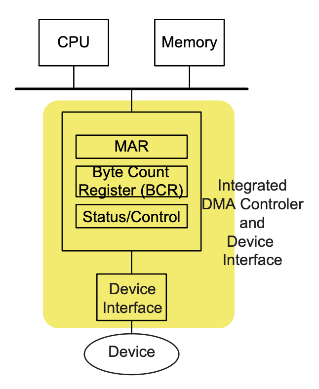
The DMA controller consists of 3 registers that allow it to act as a controller on the bus:
- The
MARcontains the address of the next byte of memory to be transferred. During a transaction initiated by the DMA controller, the contents of this register will be driven to the address lines of the system bus as it is fulfilling the same role as theMARdid in the CPU. - The byte count register (
BCR) holds the number of bytes left to be transferred in this block. Recall that DMA is only used when a number of consecutive bytes need to be transferred to the same destination. - The last register is the
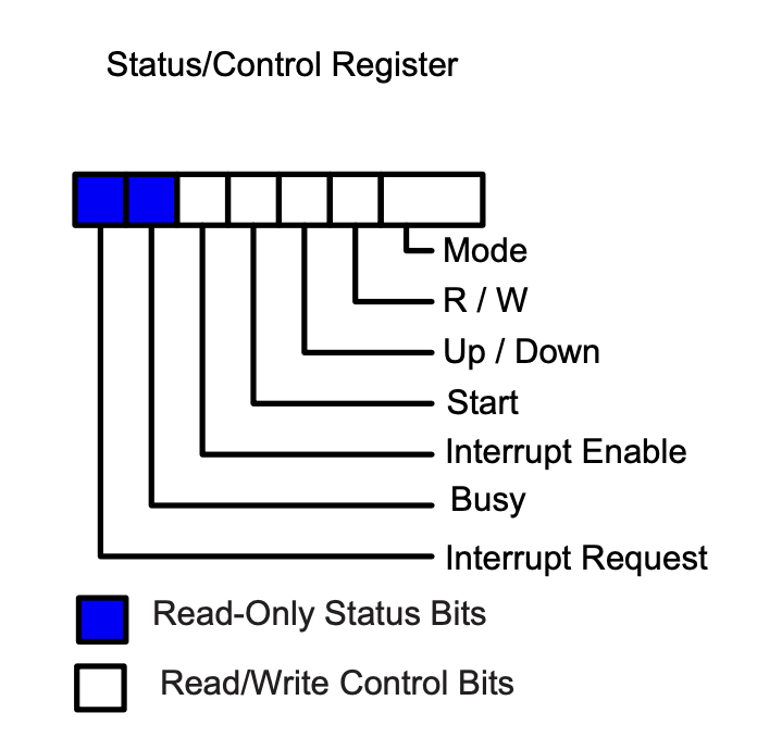
status/controlregister. Some of the bits are read only and used by the device to share information with the CPU, while others can be written by the CPU to configure the operation of the interface. The bit map of this register is shown on the right below, where the purpose of each field is:Mode: Number of transfersR/W: Direction of transfer from controller’s perspectiveUp/Down: How to change theMAR(i.e., increment or decrement)Start: Start the transferInterrupt Enable: Enable/disable interruptBusy: Synchronization bit for processing one block of dataInterrupt Request: Interrupt pending asserted after processing one block of data
Transfer Modes
The Mode bits in the status/control register determine how many transfers can take place per bus controllership. In this course, only two modes are considered.
Cycle stealing mode only allows the transfer of 1 byte (word) per bus controllership. As a result, there may be an excessive number of arbitration cycles required to transfer the complete block of data.
Alternatively, burst mode mode can be used which allows multiple transfers per bus controllership. This mode permits the transfer of (up to) the entire block in one bus controllership. In practice, unless the block size is relatively small (single digit number), it will still take multiple controllerships to transfer the block in its entirety. This mode has the advantage of reducing the latency caused by the high number of arbitration cycles associated with cycle stealing, but the processor may be blocked for as long as the bus is required by the I/O device to transfer some/all of its data.
There is a significant trade-off that must be made when using burst mode. As a result there are often constraints on the number of transfers that may be permitted in one burst. This does not limit the size of the block. During a burst transfer the CPU is prevented from accessing anything on the bus. As a result, if the instruction memory is on this bus, then any requests for interrupts will be deferred until the end of the burst transfer. The length of a burst is usually constrained by the following:
- The amount of data available to be transferred. If the device has produced 100 bytes of data, then the maximum burst length would be 100 transfers (assume one-byte transfers), even if the actual block size was 1000 bytes. The completion of the burst does not (necessarily) signal the end of a block.
- The number of bus cycles that the processor is willing to give up the bus. Some processors are designed in such a way that they cannot stop for more than cycles, meaning that they must continue processing within a limited window of time.
- There may be some other limits on the burst length such as limits on the consumer side or limits on the latency that some other part of the system can tolerate.
Integrated DMA Data Transfer Sequence
During system startup, there will likely be some global initialization required to enable the DMA hardware and set some configuration options. This work is done once.
The process that takes place for each block of data to be transferred using the simple model of the integrated controller is as follows:
- CPU loads DMA controller (DMAC) with starting memory address (in the
MAR), the byte counter (in theBCR), and control values. - When the device has data ready or is ready for more data, it sends a
DMARequest. - DMAC requests the bus and waits until it is granted through arbitration.
- DMAC provides addresses and control to facilitate the system bus transaction.
- DMAC increments or decrements (depending on settings) address in
MARand decrements byte count inBCR. - If the controller is running in burst mode.
BCR0, more data is available, and max transfer count per burst has not been reached, loop back to step 4. Else ifBCR0, release bus and loop back to step 2 as the burst limit has been reached but there is still data to transfer. - Transfer is complete; release bus, synchronize CPU and DMAC.
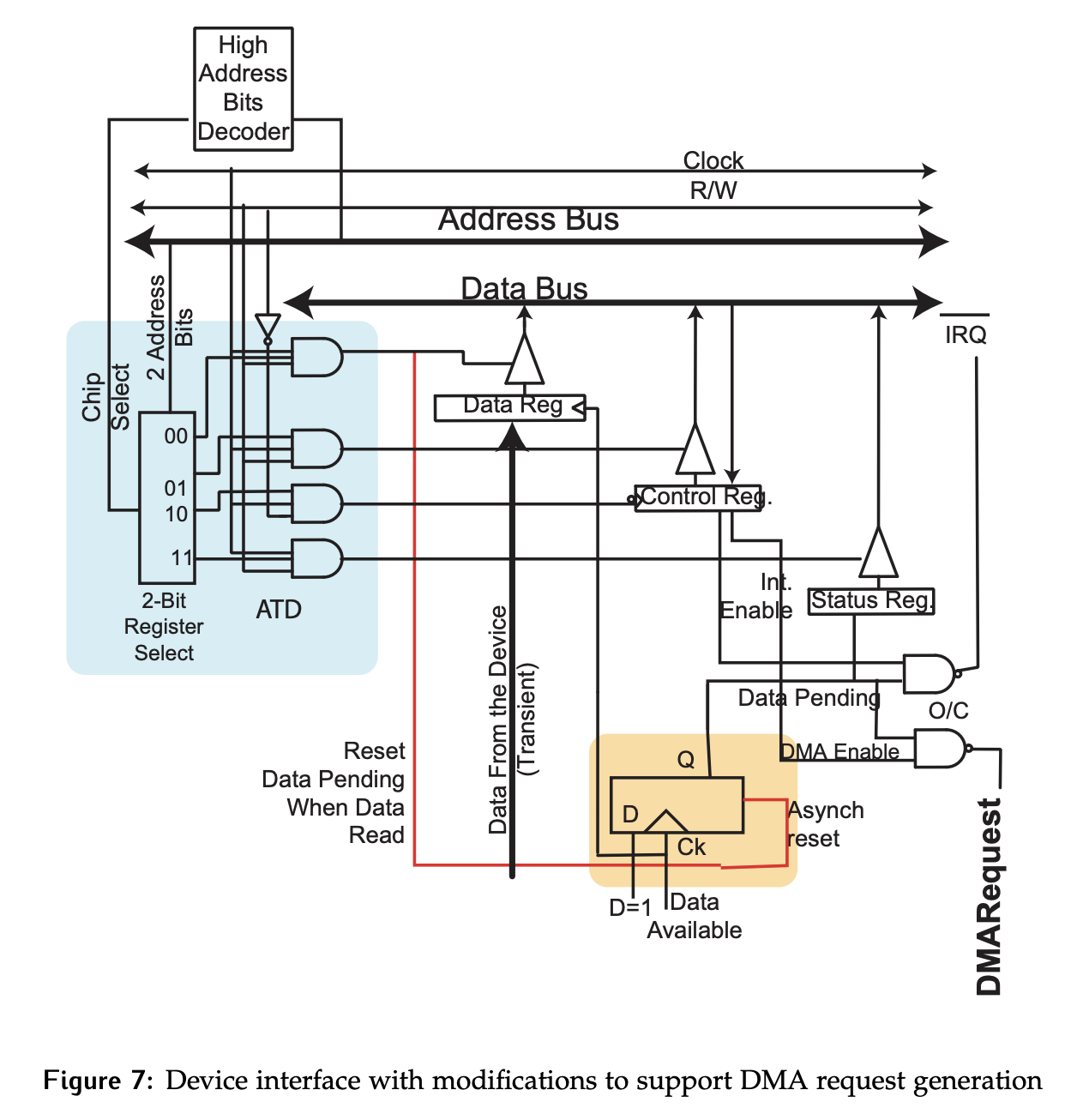
Hardware Implementation
The block transfer device interface can be modified to permit DMA transfers as shown below. An additional NAND gate has been added to produce the /DMARequest signal if DMA is enabled and data is pending. Note that only /IRQ or /DMARequest would be enabled at one time.
How would we transfer a block of 256 bytes of data in this case? The following assumptions are made:
- All global initialization has been completed
- The device interface has been set up to produce (or accept) the block of data
- We have an integrated DMA controller
- We’re using polling synchronization (for DMAC at the end of the block
The C code to configure the integrated DMA controller and transfer 256 bytes is shown here:
// Define a value array to store the bytes to transfer
unsigned char value[MAX_VALUE];

// Initialize the value array (now shown)

// Setup the DMA controller registers
dma_control = DMA_UP | DMA_BYTE_MODE | DMA_WRITE;
dma_memory_address = value;
dma_byte_count = 256;

// Initiate a DMA transfer
// NOTE: dma_control is read/write accessible.
dma_control = dma_control | DMA_START;

/* CPU executes other code in parallel here, if any. */

// CPU loops until the transfer is complete.
while (( dma_control & DMA_BUSY ) != 0 )
{
	/* Do nothing...tight polling loop. */
}
The code to transfer of 256 bytes in assembly language is shown below. The number of useless memory cycles is now reduced to . If the DMA controller completes the transfers before the CPU polls it to check if the work is complete, , in which case only 18 cycles are required. If the transfers are still in progress, the CPU will repeat the last two instructions until the work is done. This is a significant reduction from the 3330 cycles required for the CPU to complete the same transfer using tight polling.
MOVE A0, dma_memory_address      [4]
MOVE #256, dma_byte_count        [4]
MOVE #$10, dma_control           [4]
...
LOOP:    AND #$08, dma_control   [4]
BEQ LOOP                         [2]