Let’s think about the process for the CPU to move a piece of data from a register in an interface to memory. We can then compare this to DMA approaches.
It takes two system bus transactions to complete the transfer, as illustrated below in Figure 1.
- The first is a read from the interface register, resulting in the data being available in the
MDR. - Then, there is a write to memory that transfers data from the
MDRto its final location.
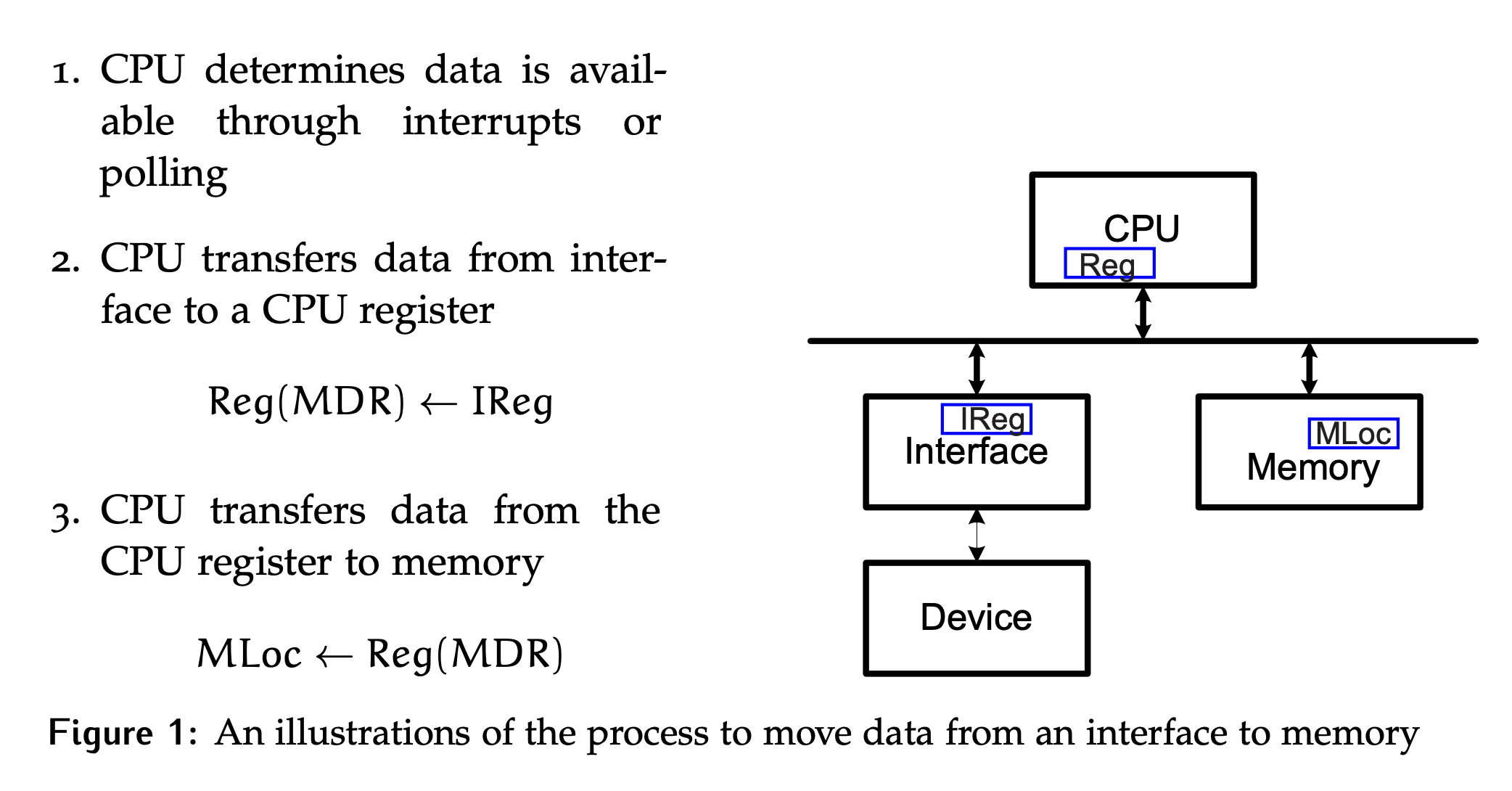
To generalize, anytime data is moved between interfaces or between an interface and memory in the system, two system bus transactions are required. The first will be a read from the source location, and the second is a write to the destination.
Block-Oriented Interfaces
Now imagine moving not just one piece of data, but an entire sequential block of data. This will require a lot of CPU time to complete. Devices that routinely transfer larger chunks of data are classified as block-oriented device interfaces. They tend to be more complex than character oriented devices, which transfer data one byte or unit at a time. The block-oriented devices often require built-in buffers to permit synchronization less frequently than every byte, which may not be possible at higher speeds and/or prevents the CPU from doing other tasks.
Hardware Support for Block Transfers
Adding support for block transfers requires some modifications to the parallel interfaces previously studied, as highlighted in orange in Figure 2. For now, assume the device is unidirectional and only provides data (read-only).
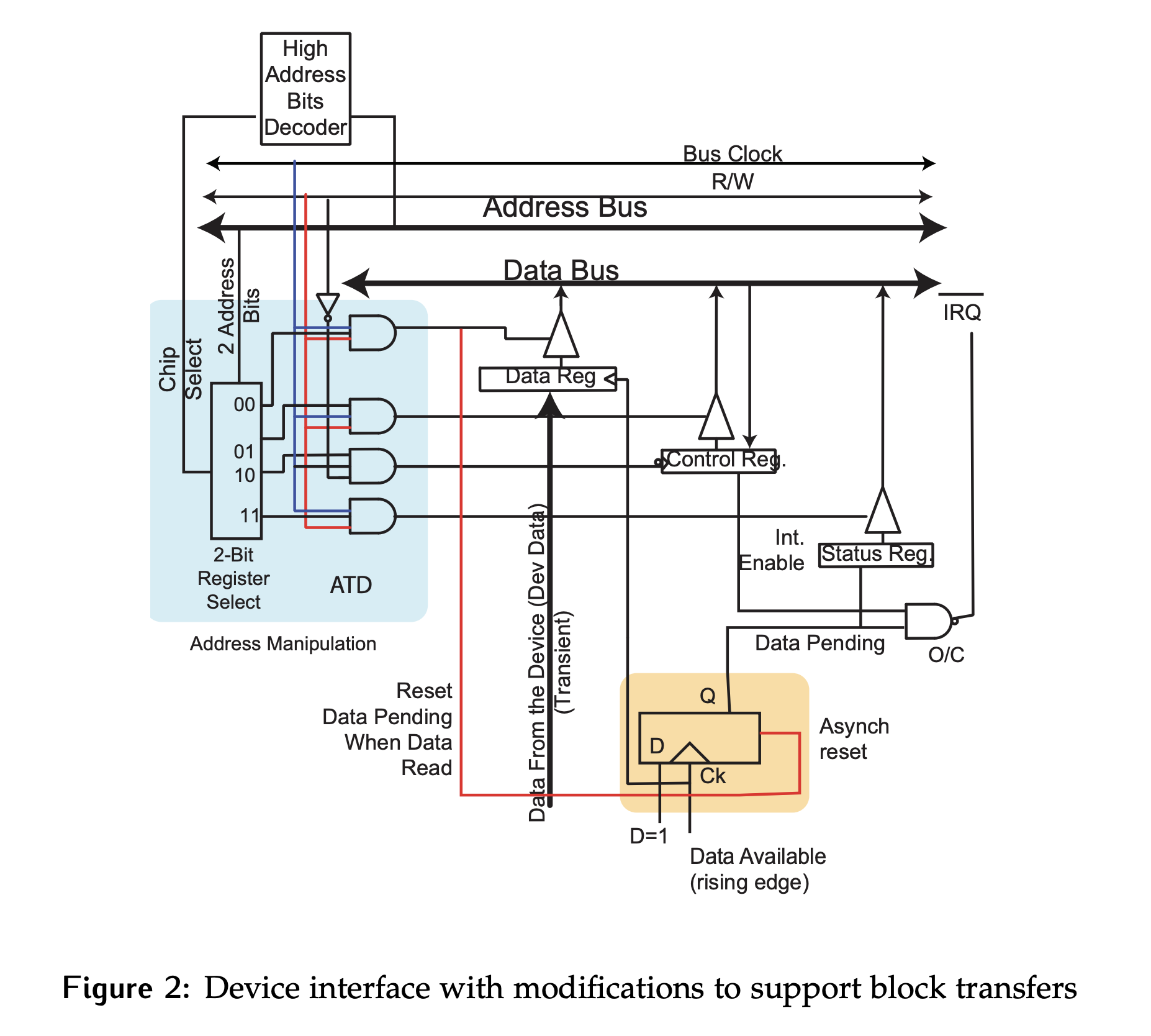
- Data is generated by the external device, and then clocked by that device.
- The interface contains a read-only status register and a control register.
- When data is clocked into the data register, the flip-flop highlighted in orange is set to
1indicating that new data is available. This line is calledData Pending, and it is saved to thestatusregister. - This
1onData Pendingcan be read by the bus controller when thestatusregister is queried. - When the
dataregister is read, the flip-flop is reset. - The output of this flip-flop is also used to generate an interrupt when new data is available, if the interrupt enable bit has been set in the
controlregister.
Block Transfer Timing
The general timing for all block transfers discussed in this chapter is shown in Figure 3.
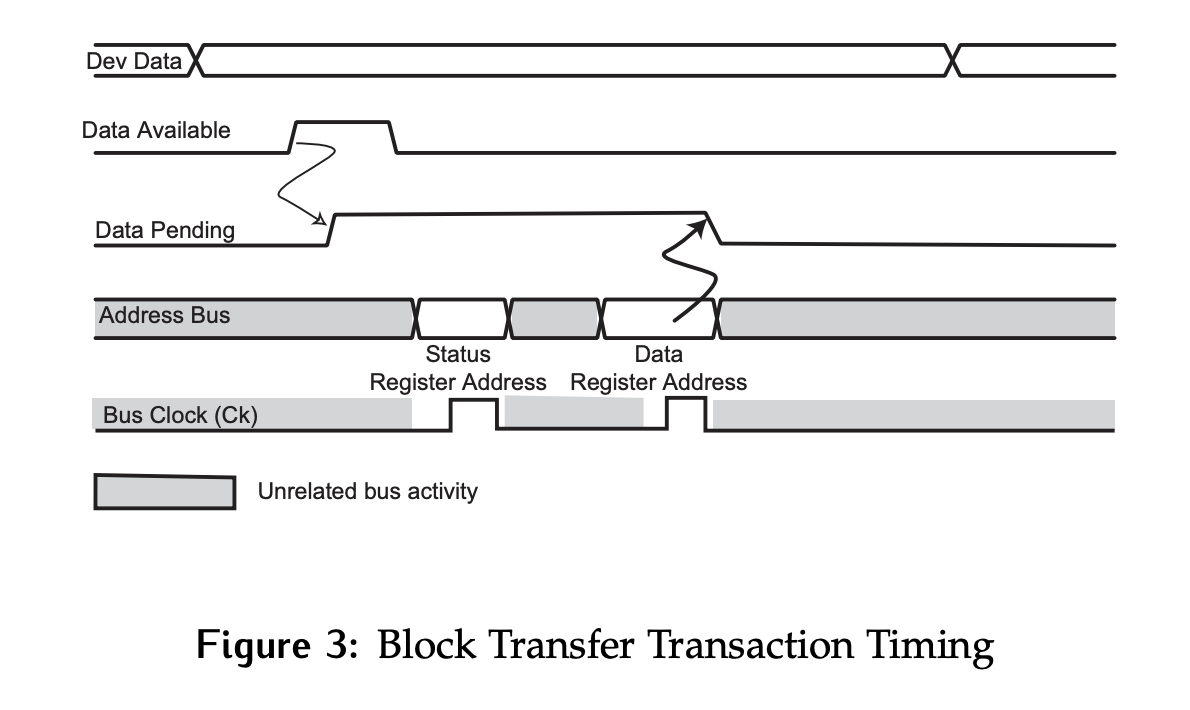
- The
Data Availablesignal will be pulsed by the device when a new piece of data is produced. - This will set
Data Pending, the output of the flip-flop in Figure 2 to1. - At some point, the CPU will read the status register and see that new data is available. This will be followed by a read of the data register to retrieve the data.
- Reading the data register will reset
Data Pending. Note that the reads of the status register and the data register do not need to be back to back.
CPU Block Transfer Methods
Before considering the finer details of a DMA-based transfer, first consider how the CPU would transfer a block of 256 bytes of data.
Assume that this is an 8-bit system, so only 1 byte is transferred per transaction. One method is to make sure the receiver is ready then transfer a byte. Repeating this 256 times will transfer the entire block as shown below. This code assumes that the Data Pending bit is stored in the MSb of the status register:
/* Loop through byte indices of 255 downto 0. */
for (int i = 255; i >= 0; i--) {
	/* Loop until the byte at index i is ready. */
	/* Assumes the data pending bit is stored in the MSb of status register*/
	teststatus: while ((Status_Register & 0x80) != 0x80)
	{
		/* Do nothing...tight polling loop. */
	}
	/* Transfer byte i into value array at index i. */
	value [i] = Data_Register;
}
The same functionality can be implemented using assembly language.
; Assume that A0 points to the next address in memory to store a value
; Assume that D0 is the counter indicating the number of values left to read
; Values shown as [2] indicate the number of memory cycles needed for the instruction.

; Initialize the counter in D0 to the transfer size.
MOVE #256, D0                     [2]

; Loop until data is ready to be processed.
Loop: AND #$80, Status_Register   [4]
BEQ Loop                          [2]

; Transfer the data to memory.
MOVE Data_Register, (A0)+         [4]

; Decrement the counter.
DEC D0                            [1]

; If not complete, continue with the loop.
BNE Loop [2]- The number of units transferred is 256.
- The number of tests at location
teststatusis unknown, but the time required is (). It can be calculated if you know the delay between each piece of data (). - Useless cycles are those that are not part of the actual data transfer/memory (bus) cycles. Assuming no cache, the number of useless cycles is , where is the number of cycles needed for synchronization.
- The smaller the time, the smaller will be.
- If a new piece of data is ready every time the device is polled, then cycles are required for the block transfer. This is the absolute minimum number of cycles, and in reality likely underestimates the resource usage.