Below we have the circuit diagram of a buck (step-down) DC/DC converter. The components of the circuit, which are assumed to be ideal, are:
- Switch S
- Diode D
- Inductor L
- Capacitor C
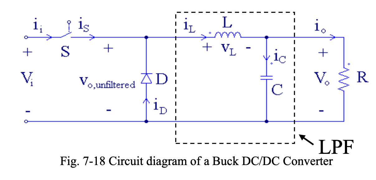
- The DC input voltage is and the output voltage is .
- represents the resistive load across the output terminals
- is the voltage across the diode .
- and C form a second-order Low-pass Filter (LPF) and are designed based on the specified percent ripple in inductor current and capacitor voltage, respectively. It will be shown later that the average output voltage is always smaller than the input voltage in a buck converter.
Operation
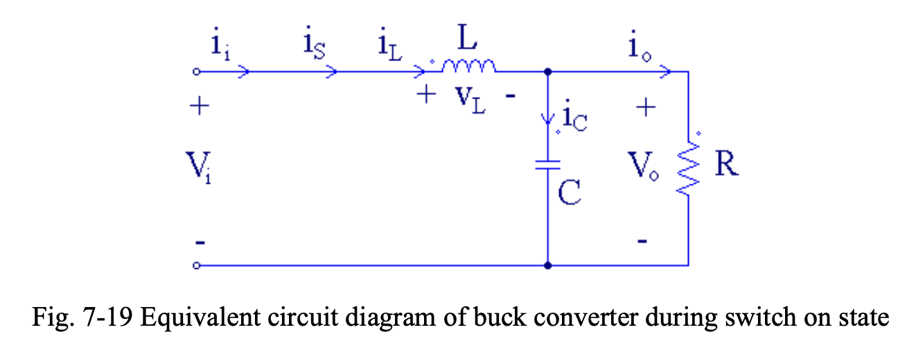
Switch On
The equivalent circuit diagram of the buck converter when the switch is on is shown below. In this state, the diode is reverse biased, and the voltage across the inductor is positive. The inductor current rises, and energy is stored in the inductor.
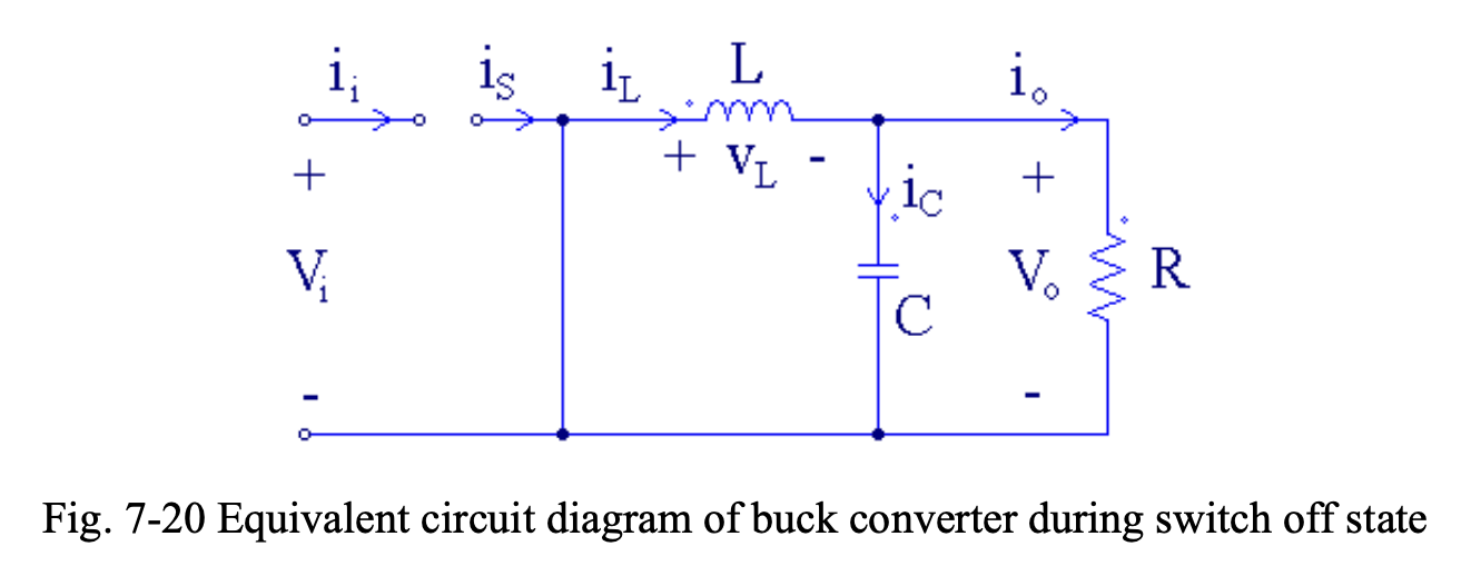
Switch Off
The equivalent circuit diagram of the buck converter when the switch is off is shown below. The inductor current is momentarily interrupted. The voltage generated overcomes the output voltage and forward biases the freewheeling diode. The voltage across the inductor () is negative. The inductor current falls and the energy stored in the inductor during switch on period is transferred to the output.
Voltage Across Diode
Figure 7-21 shows the voltage across the diode, . This is equal to when the switch is in the on state, , (since S represents a short circuit) and zero during switch off state, , (since D represents a short circuit).
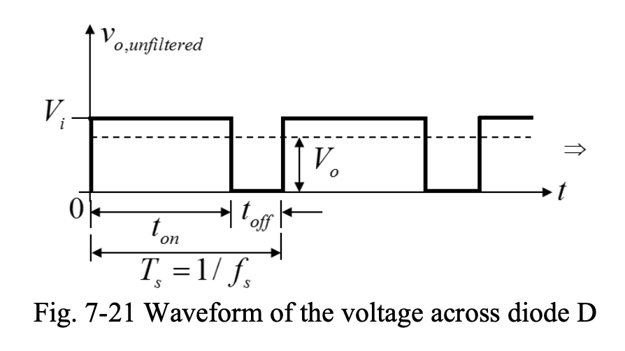
Note that
where is the switching frequency (the rate at which the switch is turned on and off) in Hz. is the average value of the diode voltage, , which is the same as the average value of the output voltage, as the LPF allows the low-frequency components of diode voltage to go through and filters the high-frequency components, that happen at the switching frequency and its integer multiples.
Thus, the average value of the output voltage can be found as follows:
where is the duty ratio or duty cycle of the switch. This relation shows that as duty ratio varies between and , the average output voltage varies between 0 and .
In other words, in a buck converter, is always smaller than , hence the name step-down or buck converter. The relation for the average value of output voltage can also be found in terms of control signal in the following way.
PWM
Figure 7-22 illustrates the PWM process. It compares with the triangular carrier signal, which is a sawtooth waveform of amplitude and frequency , and generation of switch control signal.
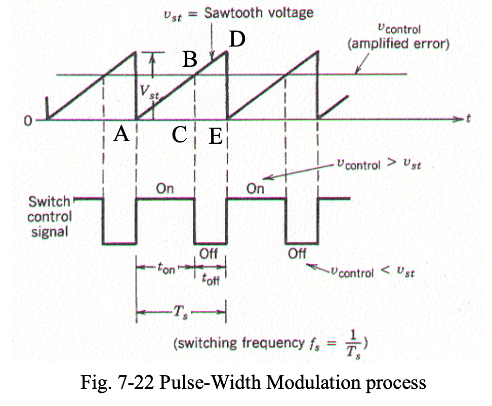
From the two similar triangles and , we can write:
Replacing the expression for duty ratio in the formula of average output voltage yields:
Thus, there is a linear relationship between and and between and . Even though the switching nature of the converter makes it a nonlinear system, there is a linear relationship between the control input and converter output voltage on an average per switching period basis. This linear relationship makes buck converter a linear amplifier, with as the input, Vo as the output, and as the gain. This allows using linear control techniques in the design of the converter.
Inductor Design
Fig. 7-23 shows the waveform of the inductor current the buck converter.
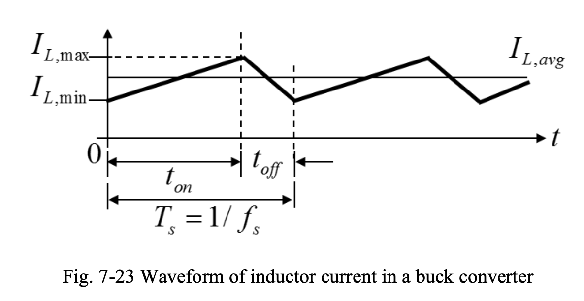
The design equation for in terms of the specified relative inductor current ripple (i.e., peak-to-peak ripple in the inductor current relative to its average value) is given without proof as:
To get a smaller inductor current ripple, a larger or higher has to be used. Thus, high switching frequency can reduce the size of .
Capacitor Design
Figure 7-24 shows the waveform of capacitor voltage in a buck converter. This is a zoom-in view of the output voltage ripple, as .
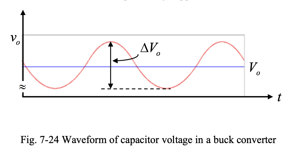
The design equation for in terms of the specified relative capacitor voltage ripple (i.e., peak-to-peak ripple in the capacitor voltage relative to its average value) is given below, without proof.
Thus, to get a smaller capacitor voltage ripple, a larger or a higher has to be used. This fact shows the advantage of high switching frequency operation that can reduce the size of .