The disadvantages of the binary ramp ADC design, particularly the variable conversion time, make it unsuitable for most practical applications. The successive approximation design vastly improves the performance by changing the search algorithm, using binary search instead of linear search.
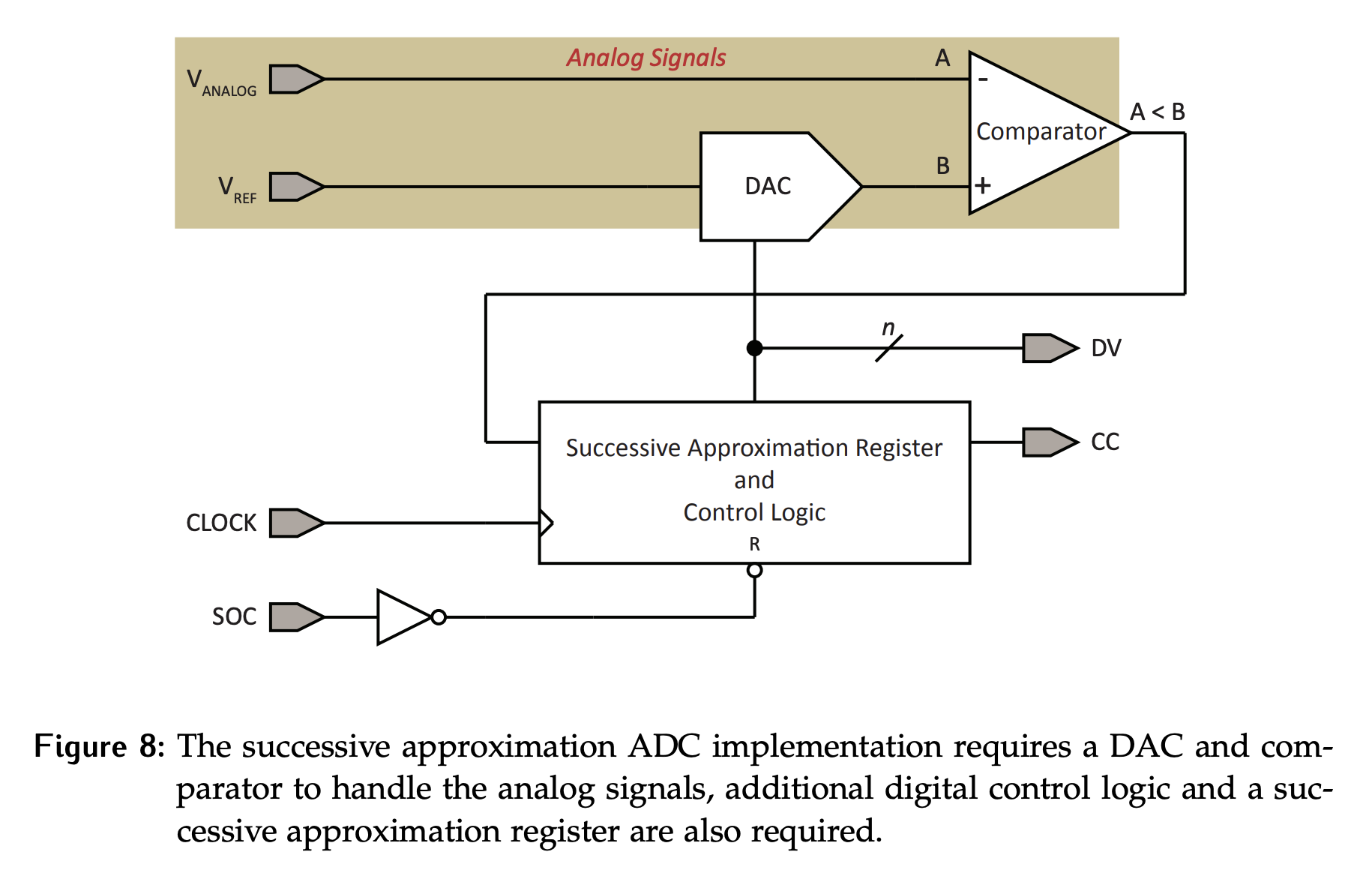
This algorithm works by starting from the most significant bit, then successively testing each bit to determine whether it should be on or off. We use a comparator to test whether the output of DAC exceeds the analog value for each input combination being tested. Once the LSB has been tested, the resulting value with be the converted digital value. Since each bit in the digital value must be tested, the conversion time is consistent. It is also relatively fast with a conversion time for bits of cycles, compared to a worst case of for a binary ramp design. It provides a persistent converted value using the implementation shown in Figure 8.
The successive approximation converter is biased low since bits are only set if the value output by the DAC is less than the analog value we want to convert. Thus, we cannot overestimate and can only underestimate.
Operation Procedure
- The Successive Approximation Register
SARcontains bits that determine the digital valueDV, which is used by the ADC.SARbits are numbered to , with being the MSB.- We use
Xto track the MSB, starting by initializingX = [n-1].
- All bits in the
SARare set to zero, settingDVto zero as well. - Set the MSB of
SARto1, so the MSB ofDVis set to1as well. UsingX, we would haveDV[X] = 1.- For example, if we have a 4-bit system, we have
SAR = DV = 1000.
- For example, if we have a 4-bit system, we have
- The DAC converts the
DVto an analog voltage. - The comparator compares this analog voltage to the input analog voltage.
- If the comparator output is high, (DAC is higher), we clear the MSB back to
0. - If the comparator output is low, (DAC is lower), we keep the MSB set to
1. - Thus, ==the bit only remains
1if we are NOT overestimating.== This is why SAR is biased low.
- If the comparator output is high, (DAC is higher), we clear the MSB back to
- Move to the next most significant bit by decrementing
X. Go back to Step 2, set the next most significant bit to1, generate analog voltage with DAC and compare.- Now, we would either be testing
1100or0100, depending on the output of the comparator.
- Now, we would either be testing
- Repeat this until we reach
Xhas been decremented to0.

Algorithm Example
Recall that the idea behind the binary search algorithm is to start by checking the middle value:
- If it exceeds what you are searching for, the desired item must be in the bottom half of the sorted data.
- If it does not, the item being sought is in the top half. Repeat. Successive repetitions cut the search space in half each time.
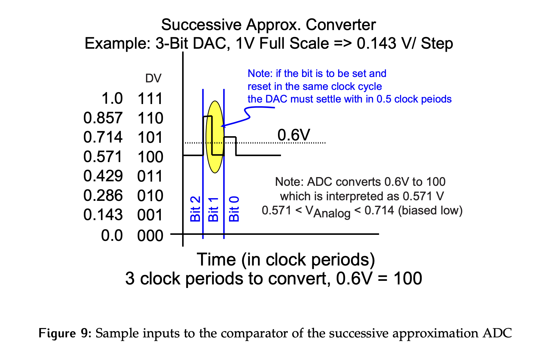
To see the algorithm in action, consider Figure 9 where the inputs to the comparator are illustrated for a 3-bit converter. The analog value to be converted is 0.6 V. Each cycle is divided into two phases: set and check.
- Initially, the SAR will be set to 000.
- At the start of the first cycle, it will be set to 100. The resulting output of the DAC is less than the analog signal, so the bit remains set.
- In the second cycle, the middle bit is tested by setting it, so 110 is the new DAC input. In this case, the DAC output exceeds the analog voltage, so the bit is reset during the second half of the cycle making the DAC input 100.
- At the start of the third and last cycle, the DAC input is set to 101. The analog value has been exceeded, so the bit being tested is once again turned off, making the final DAC input, and therefore the converted value, 100.

Software Implementation
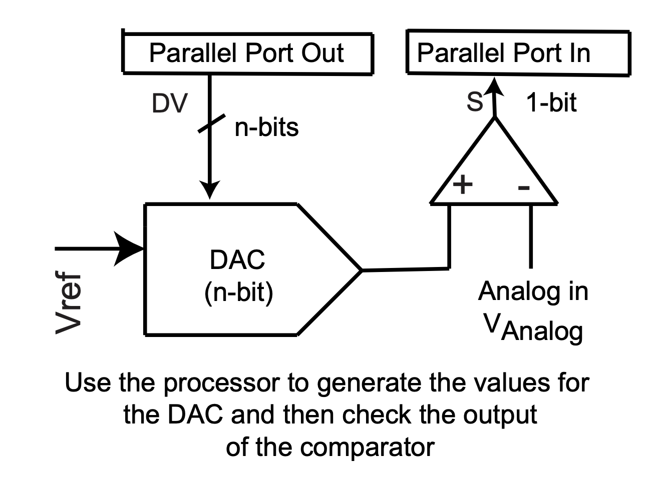
Like the binary ramp ADC, it’s also possible to implement this converter in software, coding the algorithm while keeping the analog components of the hardware. The required hardware is shown in Figure 10 while sample code for the algorithm is in Figure 11.

/* Let n store the resolution of the DAC in bits. */
/* Let DV memory map to the input of the DAC. */
/* Let S memory map to the output of the comparator. */
/* Start with an unsigned value of 0. */
DV = 0;

/* Loop over each bit from largest to smallest. */
for (i=n-1; i>= 0; i--) {
	/* Set the current (ith) bit to a value of 1. */
	DV = DV | (1 << i);

	/* Sleep, if necessary. */

	/* Check if DV is too large. */
	if (S == 1) {
	/* Reset the current (ith) bit to a value of 0.*/
		DV = DV & ~(1 << i);
	}
}
Behavior and Timing
The time for each cycle is largely driven by the speed of the DAC. The cycle must have sufficient time for the DAC output to settle when the input changes from 0 to setting the MSB and back again.
The total conversion time can be improved by observing that the DAC output does not have to change very much as the conversion progresses, thus it may be possible to clock the SAR faster as the bit to be tested changes, although the extra hardware or logic required to do this may negate the savings.
Advantages:
- Simple to implement (H/W or S/W)
- Fixed conversion time
- Glitching is eliminated as only one bit changes at a time
Disadvantages:
- Still requires multiple clock periods for a conversion
- Slower than a binary ramp ADC for very small analog input voltages