In a binary ramp ADC, a comparator is used to determine if the output of the DAC is greater than the analog signal to be converted. The binary ramp ADC is biased high; it doesn’t stop conversion until its DAC output exceeds the input analog voltage, inherently rounding up to the next quantization level.
Operation Procedure:
- Processor starts conversion by asserting the start of conversion (
SOC) signal. SOCresets the counter and the flip-flop.- Free-running clock increments counter when enabled. As the counter increases, its value is saved in
DV. - The DAC takes the current digital value
DVand outputs a corresponding analog voltage. - The comparator continuously checks whether the DAC output voltage (which is increasing as
DVincreases) has exceeded the input analog voltage. - When DAC output exceeds the analog voltage, the comparator clocks a Logic 1 into the flip-flop, indicating that the correct
DVhas been reached. This completes the conversion and assert conversion complete (CC).- Recall that the comparator outputs
1if and0if
- Recall that the comparator outputs
- When the processor detects
CC, it reads the currentDV, which now represents the digital equivalent of the input analog voltage.
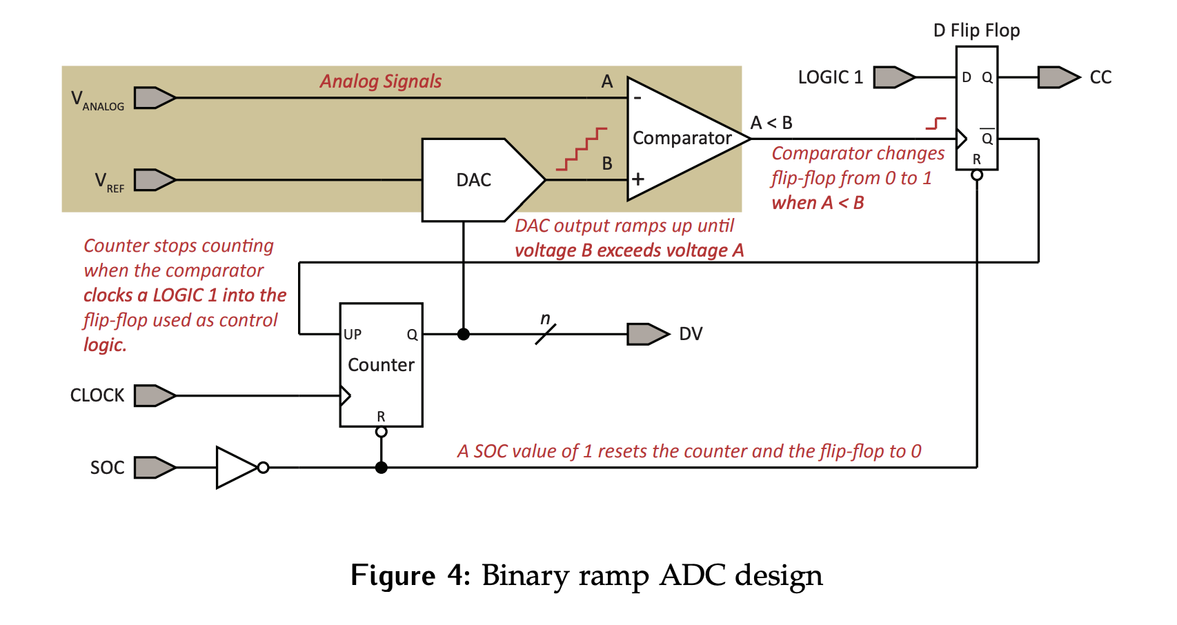
The binary input to the DAC is fed by a counter that was reset to 0 by the start of conversion signal. As the counter increments, each analog output of the DAC is compared to the analog signal to be converted. An example of the inputs to the comparator vs. time is shown in Figure 5.

Eventually a tipping point will be reached, where the output of the comparator flips from 0 to 1 because the DAC output now exceeds the analog input. The output of the comparator is fed to the clock of a flop that was also reset by the start of conversion signal to 0, so this transition in turn causes the output of the flop to switch from 0 to 1.
This will do two things: set conversion complete and stop the counter. The value at which the counter was stopped is the digital mapping of the analog input value. Since this counter will not restart until the converter is reset by a pulse on the start of conversion signal, the data is persistent and the value in the counter can be fed directly to the read data tri-state in the parallel interface to make the data visible to the CPU.
Software Implementation
It is possible to implement the digital portions of the converter hardware in software. The analog components cannot be replaced, meaning a software driven converter will still require a DAC and comparator. The functionality that was previously provided by the flip-flop and counter can be implemented in the software algorithm.
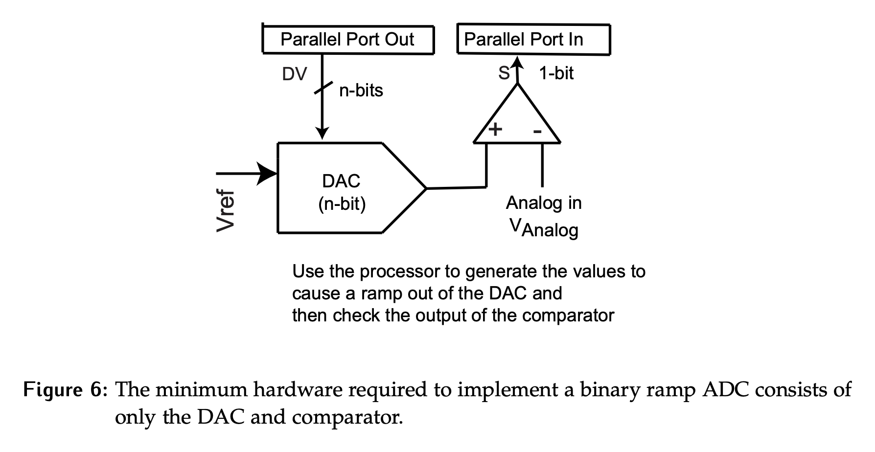
/* Let n store the resolution of the DAC in bits. */
/* Let DV memory map to the input of the DAC. */
/* Let S memory map to the output of the comparator. */
/* Start with an unsigned value of 0. */
DV = 0;

/* Sleep, if necessary. */

/* Loop while conversion not complete and the */
/* maximum value has not been reached. */
while ((S == 0) && (DV < pow(2,n)-1)) {
	DV = DV + 1; /* Sleep, if necessary. */
}

/* DV now stores a representation of the analog value. */
Behavior
Regardless of whether the functionality is implemented in hardware alone or a combination of hardware and software, there are some observations on the behaviour of this design that can be made.
The conversion speed will be a function of both the speed at which the DAC settles and the analog input voltage to be converted.
- DAC settling time is fairly constant
- Total conversion time will vary depending on the value.
- For a value close to the minimum input, the conversion will be done quickly
- For a value close to the maximum of the voltage range which will take a comparatively long time (up to clock cycles where is the resolution of the DAC)
- This is not ideal for practical systems as the conversion times will be unpredictable.
Also important to note that DAC overshoot may cause premature triggering of flip-flop.