ADCs require a stable input voltage during conversion. For our purposes, we define “stable” to mean that the value remains within for the time required to perform the conversion. The sample and hold circuit can can be built using two unity gain buffers, a capacitor and a transistor (used as a switch) as shown in Figure 5.
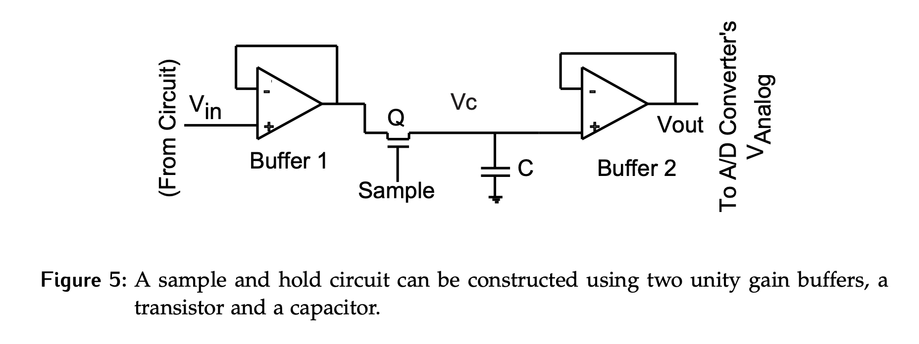
Recall that op-amps have very high input impedance (no current in) and very low output impedance (can easily source or sink current). Unity gain buffers isolate their input signal from their output by ensuring current draws at the output aren’t changing the input value.
- Buffer 1 isolates the analog circuit from when is on.
- This ensures that the sampling process does not load down or interfere with the analog input . It provides a high input impedance to the signal source and a low output impedance to drive the capacitor .
- Sampling phase: When is on, tracks .
- When is on, the capacitor is directly connected to the input voltage through Buffer 1. The voltage across , , quickly charges to match . Buffer 1 allows to follow closely without loading the input.
- Hold phase: When is off, retains the most recent level.
- Buffer 2 isolates the converter from .
- This ensures that the held voltage is not affected by the input impedance of the ADC or any subsequent circuitry. It provides a high impedance to the capacitor, preventing it from discharging, and a low impedance output to drive the ADC input. This isolation ensures that the voltage remains stable and accurate for conversion.
- Therefore, retains the most recent value and can be used as the ADC input signal.
Errors
In reality, there will be errors introduced in the sample and hold circuit. These can be considered by breaking the cycle into 4 time periods:
- During sampling
- During the sample to hold transition
- During hold
- During hold to sample transition
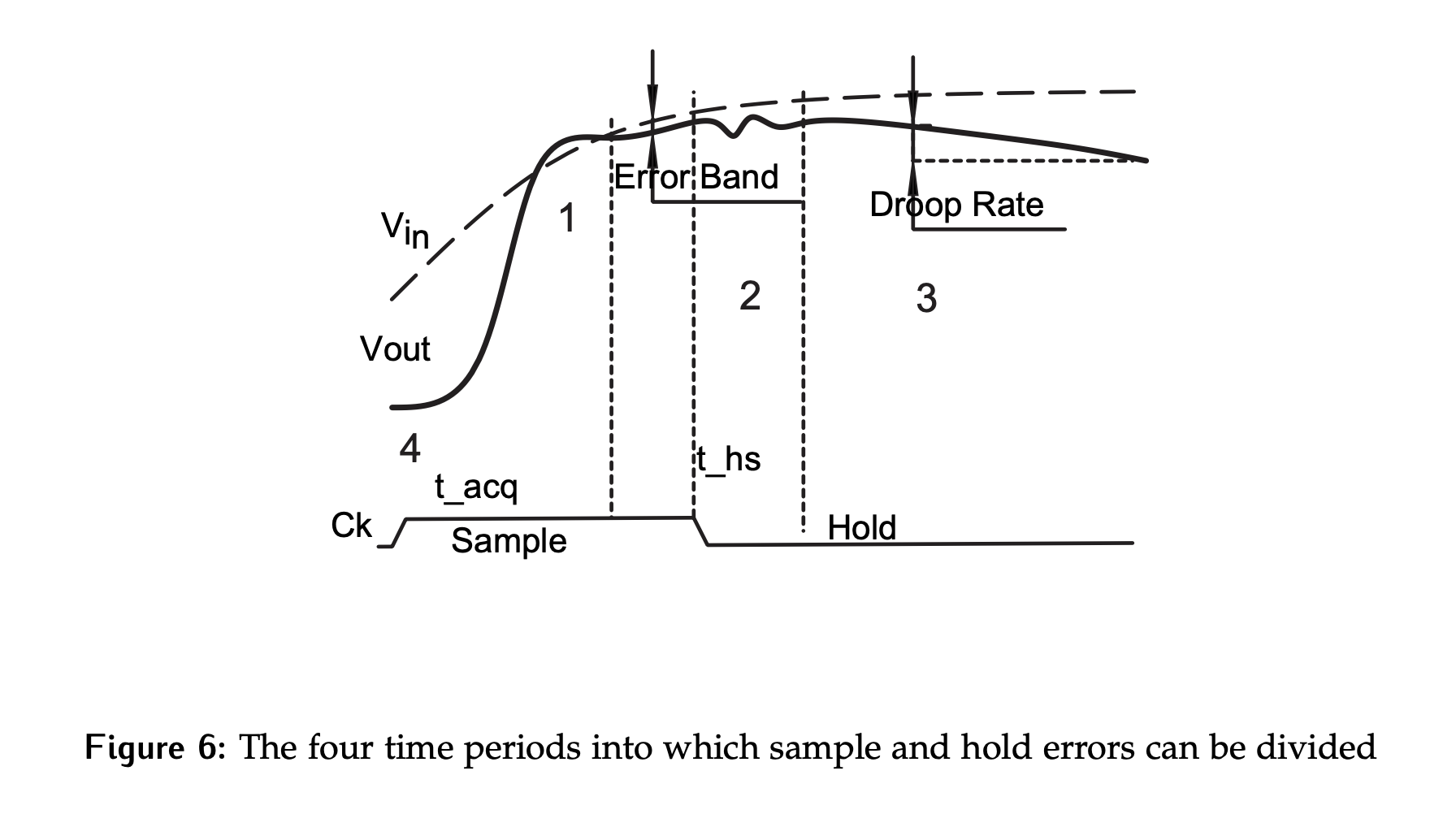
During Sampling
During sampling, errors are largely due to the input unity gain buffer:
- The op-amp may not actually have a gain of 1
- There could be an offset when an input of is applied
- Op-amp may not be perfectly linear
- There will be a time delay between the changes in the input signal and updating of the buffer output.
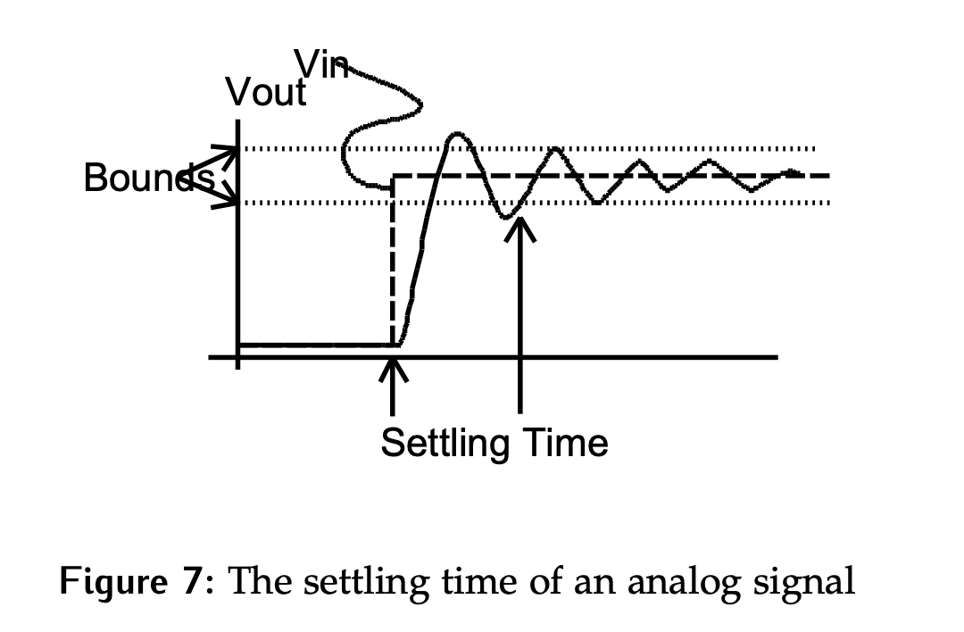
The sampling time of the circuit is also largely determined by the input buffer. The settling time is the time to attain a good estimate for the final value given a full scale step at the input (to within a specified error). In this case, it is the time to couple the voltage across the capacitor (through the two buffers) to the A/D input.
During Sample-to-Hold Transition
The sample to hold transition is a very short time period but can still introduce additional error. Using the design presented here, it is the time during which the transistor, , is turning off. Ideally, the transistor would transition instantly from full on to fully off, but reality is it takes time; this is known as the sample and hold aperture time and is marked as below.
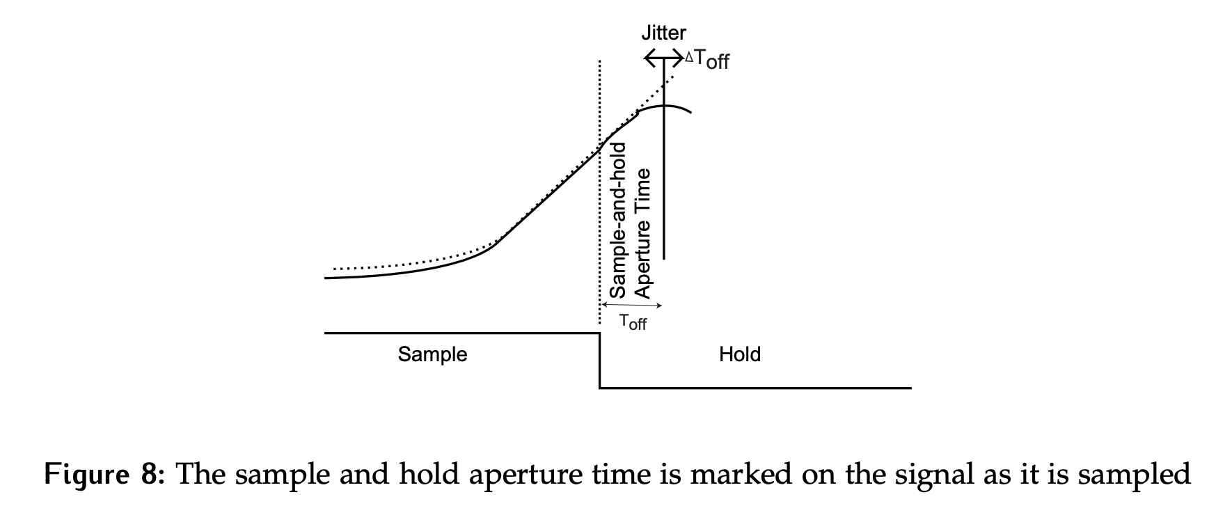
While the transistor is changing states, will not perfectly track , which may contribute to the sample-and-hold offset.
There will also be variation in exactly how long the transistor takes to turn off during the sample to hold transition from one sample to the next. This variation is typically quite small, and can be referred to as the sample and hold aperture uncertainty or jitter as marked above. Some sources of jitter are:
- Variables in the delay in turning off
- Variation in sample/hold transition
- Variation in either of these caused by changes in temperature
What is the significance of this if it only introduces a tiny potential offset? It’s most important if we are attempting to sample a signal at regular intervals, . In this case, we cannot miss a sample by the time required for the signal to change by more than a fraction of the LSB value.
Jitter Example
Consider the following scenario: We need to sample a 10 kHz signal using a 10 converter. How much jitter can be tolerated?
Assume that the uncertainty occurs at the maximum rate of change point, using from here. Then, we have:
Thus, the sample and hold aperture uncertainty or jitter time cannot be more than .
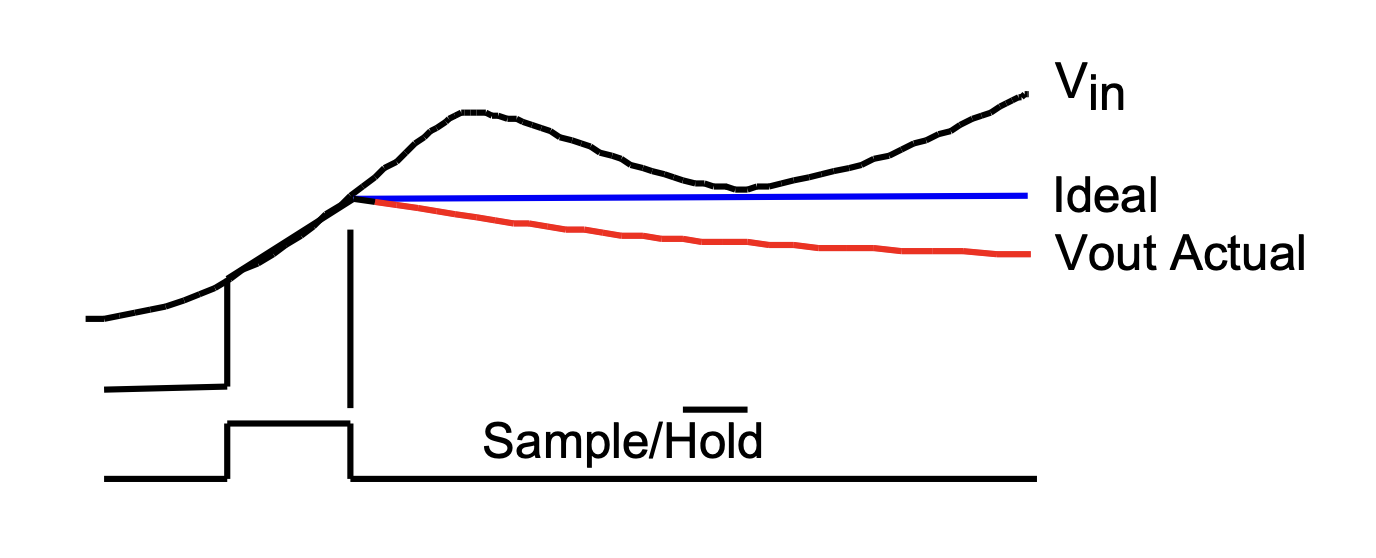
During Hold Time
Once the transistor is fully off, we’ve entered the hold phase. At this point, errors are largely due to leakage on the capacitor causing it to discharge compared to the ideal, as shown below. This drop in capacitor voltage is called droop. It is caused by discharge of due to:
- Input bias currents (in the output buffer)
- Leakage through the transistor switch
- Leakage across
Hold to Sample Transition
The final time period to consider is the transition from the hold phase back to the sample phase. The time required before the capacitor voltage is within a specified percentage of the final value is called the acquisition time. This is distinct from the settling time which worries about the voltage into the ADC, as opposed to the voltage across the capacitor. This time is marked as on Figure 6.
At times, the input and stored values may appear to be close but still there may be transients when sampling starts, largely due to stray inductance and capacitance that may be present in the circuit.