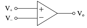
So far we’ve been operating using some ideal Op-amp Assumptions. Things can be different in real life.
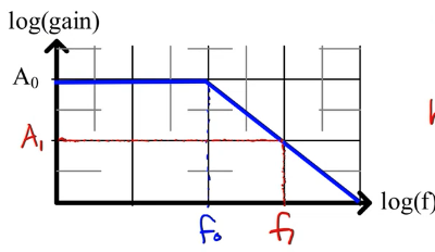
Open-loop Differential Gain
This is called or . It’s defined as:
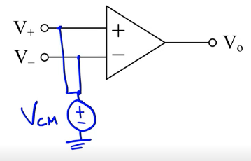
Common Mode Gain
If we apply a voltage that is common to both terminals, we actually get some output, such that is a function of . (“CM” means “common mode”, as in common to both inputs).
In an ideal scenario, adding a common voltage to the two nodes shouldn’t make a difference. However, there is always going to be a slight difference. If I add some voltage to one side and there is this slight difference, it will seem like I just applied a positive difference to it even though I didn’t. The reason is that transistors are highly reactive.
Governed by:
This value tends to be many orders of magnitude smaller than .
Common Mode Rejection Ratio
We can quantify the effect of common-mode gain by using a CMRR. In general terms, a rejection ratio is:
For CMRR, this is:
This is usually in units of decibels.
DC Offset
If we apply , you do not get due to manufacturing randomness.
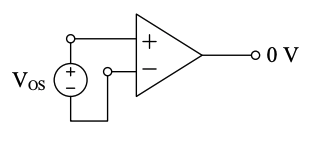
We use the concept of , defined as:
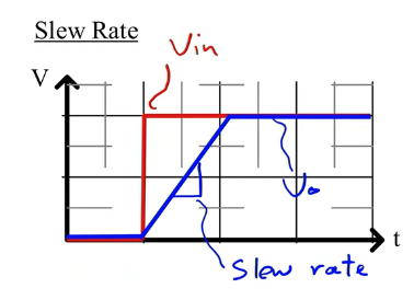
Slew Rate
Slew rate refers to how fast an output can change in response to a step input ? Did this in MTE 220 Lab 1.
Gain Bandwidth Product
This refers to a tradeoff gain to achieve higher frequencies, such that: