Summary
- Memory mapped I/O is how we communicate with hardware. Everything on the chip is accessible via memory addresses. These addresses are called “registers”.
- The bits in the register configure the peripheral. These registers are basically giant bit fields. We read the datasheet for our chip to understand what to set them to, then we use bitwise operations to actually do that.
- The register addresses are just pointers: don’t think too hard about it. Think of it as finding the address for an integer and then writing a value to that integer.
- Without the datasheet this is meaningless: none of this is obvious or straightforward at all. The process of learning to use a single peripheral can take days, weeks, or even months if the peripheral is complex enough. We usually rely on libraries for really complicated peripherals, but someone has to write those libraries!
Pin management
Look at the bare metal of the IC – there are wires coming off of it. These wires are known as “pins”. An IC only has so many pins, which is often not enough for all features of the chip to be used at once. Some pins do multiple things, but never at the same time. Pins therefore must be configured. This is a more general problem than just pin management.
Info
MMIO is a paradigm by which we access various chip settings, peripheral circuitry, and other settings using only memory addresses. It reduces the complicated tasks of interfacing with hardware to simpler pointer operations.
Peripheral
What exactly is a peripheral?
- The core of the CPU is the set of circuits that make the computer what it is (instructions, buses, etc.)
- Any other circuit that the CPU interacts with is a peripheral.
Examples:
- Secondary storage is accessed through a PCle peripheral
- UART on Cortex M4
GPIO
To best get the idea of MMIO across, we avoid abstraction and learn about digital input and output (“General Purpose IO”, or GPIO) along with MMIO. GPIO is the physical wires that read or write digital voltages on our chip, and is programmed via MMIO techniques.
Anatomy of Memory-mapped Peripherals
Memory-mapped peripherals are controlled via sets of registers, which are accessed via memory addresses that are fixed for a given chip. We can break these registers into two pieces:
- Peripheral specific: Only used by the peripheral and contain both settings and operating registers. The settings registers configure the peripheral (might have many modes). The operations registers typically make the peripheral do what it is supposed to do (handle data transfers, etc)
- Global: Chip-specific and handle basic functions like ensuring power reaches peripherals, and are able to access clock signals.

BASE + OFFSET Addressing
In a chip’s datasheet, we can see the addresses of these peripheral registers. We are accessing and modifying the registers as though they are pointers, so we need to know and manipulate the addresses.
Previously, we used keywords like new to get memory addresses from the OS:
int* x = new int(10); // allocate an array of 10 intsThe OS would find the memory location for us. But who writes the OS code that finds those addresses for you? Also, when you are dealing with registers you know the address and you have to write it into your code. This is typically done by casting. Memory addresses are, fundamentally, just unsigned integers. They might be constants (e.g. registers) or variables (e.g. memory allocation program), but they are just integers. Therefore, if we know what the integer is, and we have sufficient privileges in the computer, we can just go ahead and set a pointer to have any address we like as long as we ensure the data type is correct.
For example, if we want an integer pointer with address 0x05, we have to cast it as a constant.
int *x = 0x05 // No, because 0x05 is an integer, not a pointer
int *x = (int*)0x05 // OK!
Many peripherals are duplicated in the computer, typically because it is useful to have several copies (for instance, several USB ports). To begin our running example with GPIO, there are several peripherals called GPIOA through GPIOF (and usually just referred to as GPIOx), each controlling different IO pins. The GPIOx peripherals are all the same, so rather than list every address for every duplicate register, the manufacturer has chosen to list a BASE address, which is where the first peripheral of a given type has its registers, and OFFSET addresses, which is the offset, in bytes, of a specific register. To access a particular register, you do the following:
unsigned int* REG = (unsigned int*)(BASE + OFFSET)Note how we have to first add the BASE + OFFSET before doing the cast – – the BASE and OFFSET are byte addresses, but the registers themselves are almost always unsigned integer pointers. The rules of pointer arithmetic state that you do the math then you cast, or you get very good at figuring out how byte addresses translate into other memory units
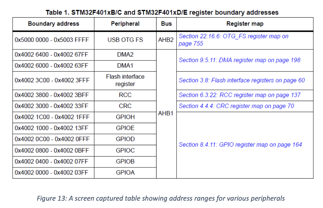
In the datasheet below, we see that each GPIOx has an address range. The BASE for the specific peripheral is the lowest address in the range:
- For GPIOA, the
BASEis0x4002 0000 - All registers for GPIOA live between this
BASEand the upper range (0X4002 03FF)
Importance of GPIO/MMIO
Unlike a general-purpose register that we learned about before, MMIO registers are basically just integers whose bits have special meaning. One bit might control which clock is being used, another bit might tell the peripheral to start or stop its operations, and yet a third and fourth might set an operating mode.
This bit-field-register idea is used because many of the settings of peripherals are binary or have only a few options. For instance, whether a peripheral is enabled or not is a single bit of information that needs to be stored. Rather than having an entire integer to store this, it is far more efficient from to store this in a single bit. The downside is that the registers and their uses can get quite complicated. Learning exactly which bit and which register does what is daunting. We are just going to look at the GPIO registers, and then we are only going to use one as a specific example. In order to learn more, you usually pick a peripheral to work with then learn how its registers are structured. This can be a lot of work if the peripheral is complex!
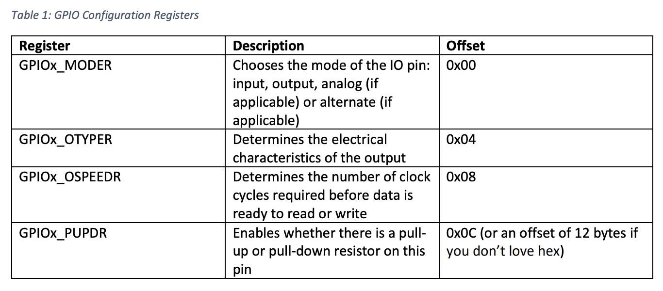
GPIO Configuration Registers
There are four registers used to configure the GPIO itself, plus a few more to configure global clock settings. The four GPIO-specific registers are shown in Table 1.
For now, we are only interested in GPIOx_MODER, we’ll leave the others to their default values. In Figure 14: GPIOx_MODER Description we can see the description of the register. Let’s learn how to read it.
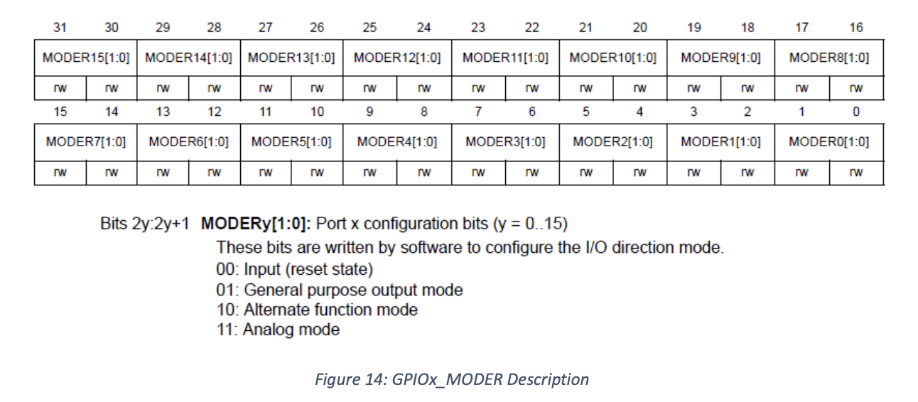
Huh? Remember that each register is 32 bits long. It turns out that our GPIO peripherals are organized into sets of 16 physical pins on the processor. This decision was not arbitrary – if there are 16 pins that lets us use 2 bits per pin to describe the type of IO that the pin does. This gives us four options:
- Input (read digital voltage)
- Output (write digital voltage)
- Alternate function (this depends on the pin, so we’ll skip this for now)
- Analog input (only some pins are physically capable of this)
Let’s say that we want to set pin 5 of a particular GPIO peripheral to an analog input, which would mean that we need to set bits 10 and 11 to 1, which would result in the mode being set to 0b11, which is analog input mode. Here is the code to do this:
#define GPIOA_BASE 0x40020000
#define _GPIOA_MODER *(uint32_t*)(GPIOA_BASE + 0x00)
...
_GPIOA_MODER |= 1<<10;
_GPIOA_MODER |= 1<<11;