One major difference between write and read transactions is where the data is coming from and going to. In this case, the data will be driven by the controller (MDR of CPU) onto the bus. The destination will be a location in the peripheral where the data is to be written, such as a register in an interface or a location in memory.
Ladder Diagram
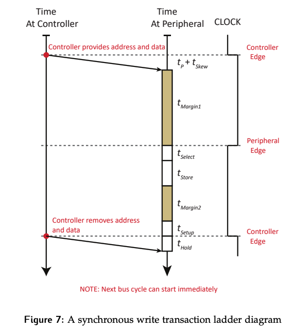
Similar to a read transaction, the controller drives the address and indicates the transaction type.
- In this case,
R/Wis set to 0.
With a write, the controller also supplies the data right away. The bus propagation delay (), which is the max of the address and data propagation times is used. This is because the CPU sets these values at the same time and therefore their propagations will overlap. There will also be skew time since both the address and data contain multiple bits.
Starting at the peripheral edge, device selection (select time ) will take place. Now the device interface will be aware of its involvement in the transaction.
Since this is a write, we don’t need to access or retrieve a specific piece of data. Instead, data from the bus needs to be available at the input to the register it will be clocked into. This is called the store time ().
- Remember that store time does basically everything but actually store the data! Clocking in the data will happen on the next rising edge.
For now, the extra time in between when the data became available at the input of the destination and when it was actually clocked in is margin time ().
Since data is to be stored in a flip-flop register, the setup time and hold time around the clock edge must still be observed.
Timing Diagram
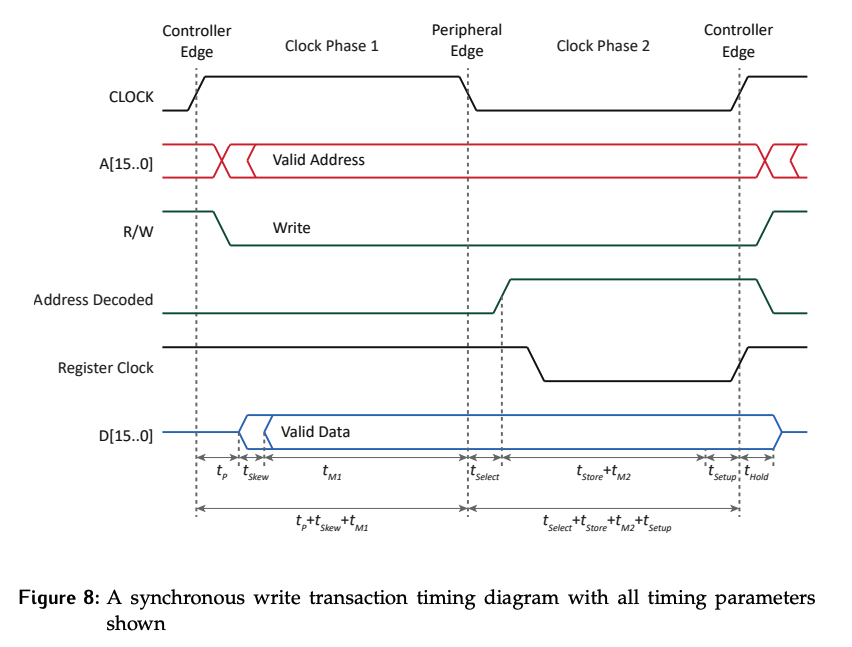
In the timing diagram, we see that there is a Address Decoded signal and a Register Clock.
Address Decoded functions identically to the read case, indicating that the target device is now aware of its involvement in the transaction.
Register Clock is the signal whose rising edge will result in the value being stored into the register in the device interface. This rising edge will be aligned with the rising edge of the clock. This signal is:
- High most of the time. This doesn’t matter because only the rising edge has any effect.
- Goes low once the device knows it has been selected and determines which specific register to store information in
- Goes back to high on the next rising edge of the clock
Consider the logic that drives Register Clock. We can’t just use the clock directly, because this would result in all registers being written to every clock cycle, which is not the desired behavior. The conditions under which data should be stored are:
- Address on the bus should be that of the registers
- Transaction is a write
- Currently in the peripheral clock phase
Putting these together gives us the Normal Clock in Figure 9. However, this signal results in a rising edge in the middle of the peripheral phase, eliminating the margin time and could potentially result in the register being clocked before is completed.
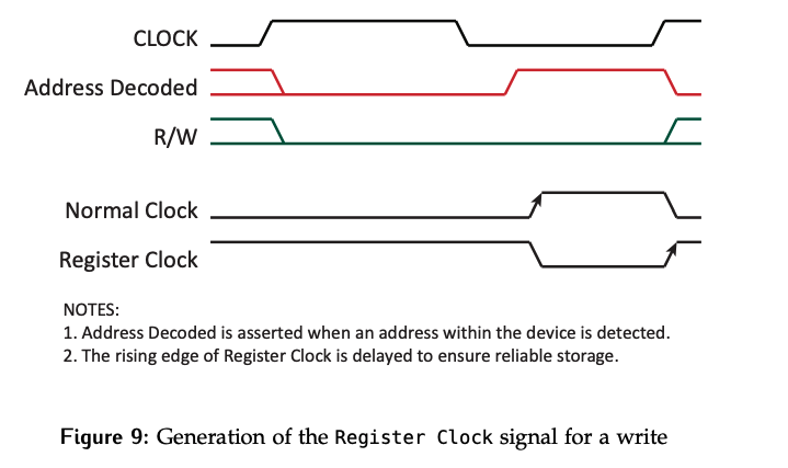
To fix this, notice that the falling edge of the signal aligns with the controller edge of the clock. Thus, we can just invert the signal to create a Register clock signal: